

Electronics ShenZhen factory for PCB assembly
- Payment Type:
- T/T in Advance, L/C or PayPal
Your message must be between 20 to 2000 characters
Contact Now| Payment Type: | T/T in Advance, L/C or PayPal |
|---|
- Fabrication data inputs: Gerber data RS-274-X or RS-274-D with aperture list and drill files Design file with Protel, PAD2000, POWERPCB, ORCAD
- Material: FR-4, high Tg Fr4, high frequency board (Teflon, Rogers, Arlon), Halogen free, rigid-flexible board
- Board thickness: 0.21-6.0mm
- Layer counts: 2-16 layers
- Surface finishes: HASL, lead-free HASL, immersion gold, gold finger, gold Plating, OSP
- Minimum line width/spacing: 4/4mil
- Minimum hole size: 0.25mm
- Minimum solder mask gap between dam: 4mil
- Maximum panel size: 20 x 30-inch
- PCBA design and making basing on samples or BOM and PCB files
- We also can reverse PCB for you according to your samples
- PCB assembly
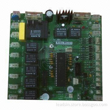
- Consumer, computer, communication, industrial, security, power, traffic control board SMD, DIP, AI OEM/ODM assembly
- Complete product including plastics, metal works, microchip progrmming and functional testing ISO9001/9002 cerfication process Small order, high-mixed accept turn-key service including components procurement, produce, quality check, package, logistics
-
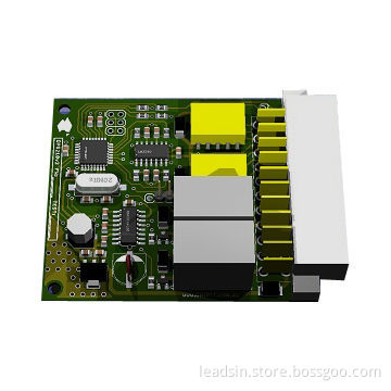
PCB Design Services and PCBA Assembly with F4 Materials and 3 Mils Minimum Insulation Thickness
-
SMT PCBA Assembly, Used in Industrial Control, FR6, 3oz Cooper Thickness with RoHS Mark
-
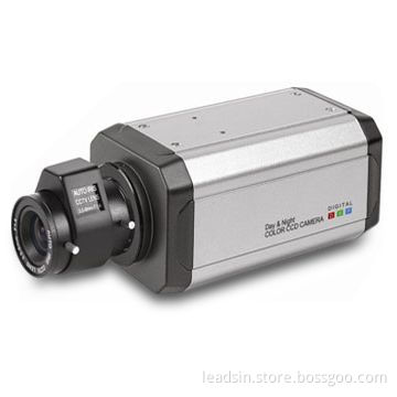
IP Box Camera/CCTV Camera with CCD Sensor, OEM and ODM Orders Welcomed
-
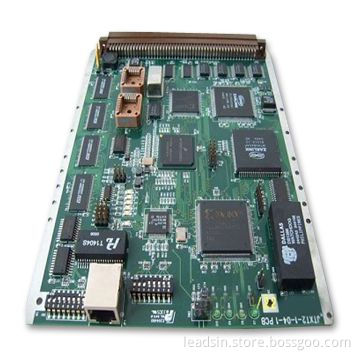
Circuit Board Assembly, Suitable for Main Control PCBA, with HASL Finish, OEM/ODM Services Provided
Related Keywords
-
PCB Design Services and PCBA Assembly with F4 Materials and 3 Mils Minimum Insulation Thickness
SMT PCBA Assembly, Used in Industrial Control, FR6, 3oz Cooper Thickness with RoHS Mark
IP Box Camera/CCTV Camera with CCD Sensor, OEM and ODM Orders Welcomed
Circuit Board Assembly, Suitable for Main Control PCBA, with HASL Finish, OEM/ODM Services Provided
PCB Assembly for Elemental Analysis, with HASL Surface Finished
Related Products-
PCBA, Manufacturer for Sound Control Product Finish, RoHS Directive-compliant, BGA SMT Placement
-
PCB Assembly with 0.075mm/0.075mm/0.075mm Minimum Line Spacing/Width/Hole
-
Circuit Board SMT Assembly, Made of FR6 Material, with 1 to 3oz Copper for Energy Saver Controller
-
PCB Assembly for Elemental Analysis, with HASL Surface Finished
-
Circuit Board Assembly, Suitable for Main Control PCBA, with HASL Finish, OEM/ODM Services Provided
Product Categories-
PCB assemblies(346)
-
Multilayer PCBs(42)
-
Electronic products OEM & ODM services(47)
-
High-density multilayer PCBs(30)
-
Telecom products OEM & ODM services(23)
-
Computer products OEM & ODM services(21)
-
Intelligent controller boards(20)
-
Security products OEM & ODM services(19)
-
PCB design services(13)
-
Contract manufacturing services(13)
-
LED work lights(10)
-
LED taillights(9)
-
Automotive LED work lights(9)
-
Rigid-flex PCBs(4)
-
Flexible PCBs(7)
-
Turn signal lights(7)
-
Stamped metal parts(2)
-
Encapsulated transformers(5)
-
Mold & tooling design services(4)
-
Injection molds(5)
-
Hardware industry mold-making services(6)
-
Cable supplies for iPhone(4)
-
Bicycle headlights(4)
-
LED lightbars(5)
-
Quick-turnaround PCBs(4)
-
Work lights(4)
-
Power banks(4)
-
Double-sided PCBs(4)
-
Polyimide PCBs(2)
-
Subsystem modules(3)
-
LED display control cards(3)
-
Medical power supplies(3)
-
Sewing machine needles(2)
-
Electronic cigarettes(3)
-
Automotive sensors(2)
-
Lightbars(3)
-
Taillights(3)
-
Double-sided flexible PCBs(2)
-
PCB laminates(2)
-
RF connectors(2)
-
Wire to board connectors(2)
-
Electronic automation supplies(3)
-
Transfer switches(2)
-
Infrared sensors(3)
-
Side-view LEDs(3)
-
LED drivers(2)
-
FM transmitters(2)
-
LED floodlights(3)
-
PCB processing equipment(2)
-
Traffic control products(2)
-
Car power inverters(1)
-
Industrial 3G routers(2)
-
Industrial computer power supplies(2)
-
Single-board computers(1)
-
Single-sided flexible PCBs(1)
-
Multilayer flexible PCBs(1)
-
High frequency PCBs(1)
-
Aluminum PCBs(1)
-
PCB multilayer laminating services(2)
-
Electronic industry mold-making services(2)
-
RCA cable assemblies(1)
-
USB connectors(1)
-
Board to board connectors(2)
-
Digital multimeters(1)
-
Membrane switches(2)
-
Membrane keyboards(2)
-
LED panels(1)
-
Joysticks(2)
-
Cigarette chargers(2)
-
Lighting controllers(1)
-
LED spotlight bulbs(2)
-
Drink machines(1)
-
Dual USB port power banks(1)
-
Nose hair trimmers(2)
-
Varifocal dome cameras(1)
-
Freeze & temperature alarms(2)
-
Bicycle rear lights(1)
-
Wireless data modules(2)
-
Car radar detectors(1)
-
Automotive battery terminals(1)
-
Automotive LED interior lights(1)
-
Car strobe lights(1)
-
FR-4 PCBs(1)
-
Power relays(1)
-
LED indicators(1)
-
Indicator lights(1)
-
Microcontrollers(1)
-
ASICs(1)
-
Motor controllers(1)
-
Educational robots(1)
-
Universal remote controls(1)
-
Digital audio decoders(1)
-
A/V receivers(1)
-
Fractional carbon dioxide laser machines(1)
-
LED table lamps(1)
-
Musical accessories(1)
-
Electronic cigarette rechargeable batteries(1)
-
Electronic smoking pipes(1)
-
Floodlights(1)
-
Gate openers(1)
-
Canister vacuum cleaners(1)
-
Window air conditioners(1)
-
Garment steamers(1)
-
Electric BBQ grills(1)
-
LED lighting controllers(1)
-
SMT machines(1)
-
Industrial steam presses(1)
-
Industrial sewing machines(1)
-
Temperature controllers(1)
-
Metal stamping(1)
-
Precision metal stamping(1)
-
Electric foot massagers(1)
-
Doppler fetal monitors(1)
-
Bluetooth handsfree kits(1)
-
Universal travel adapters(1)
-
Access control keypads(1)
-
Wiegand card readers(1)
-
SIP video doorphones(1)
-
Mobile signal boosters(1)