
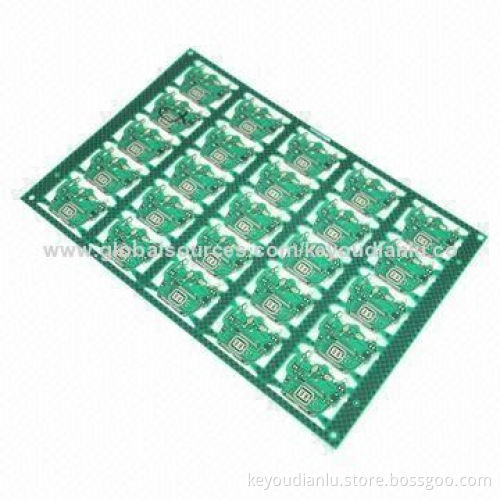
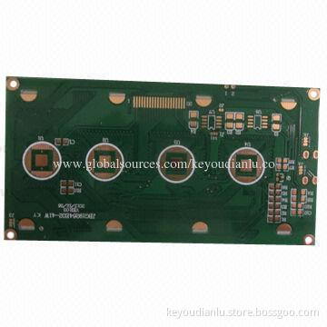
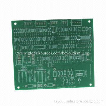
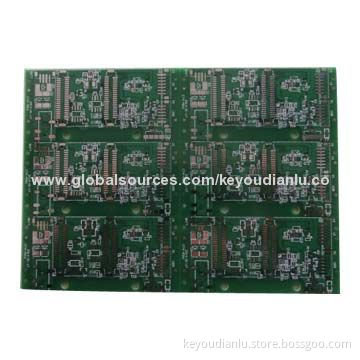
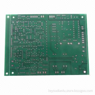
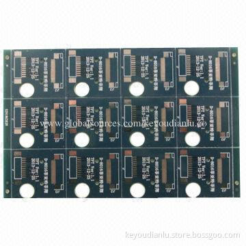
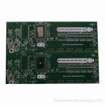
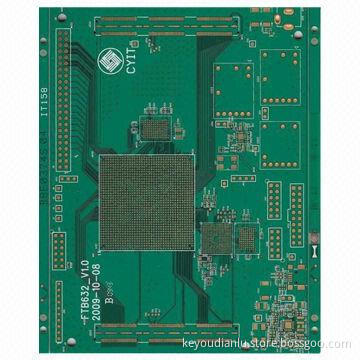
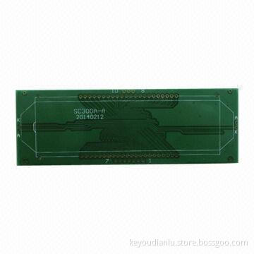
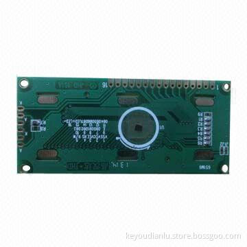
Multilayer PCB with Blind and Buried Via with Flash Gold Plating Finish
- Payment Type:
- L/C, T/T or PayPal
Quantity:
Your message must be between 20 to 2000 characters
Contact NowBasic Info
Basic Info
| Payment Type: | L/C, T/T or PayPal |
|---|
Product Description
Product Description
Related Keywords
Related Keywords
You May Also Like
You May Also Like
-
Double-sided PCB with 1.6mm Board Thickness, 1oz Copper Thickness
FR4 PCB Board, 0.3mm Minimum Hole Diameter
Immersion Gold Double-sided PCB with 1.6mm Board Thickness, 0.3mm Minimum Hole Size
Double-sided PCB, ENIG surface finish
Top Quality PCB with Double Sides, 0.3mm Minimum Hole Diameter
Related Products-
Multilayer Immersion Gold PCB, FR-4 Material, 1.6mm Thickness
-
Mech Blind Board, 0.9 Minimum Via Diameter
-
Multi-layered PCB, with Immersion Tin Finish, Used for Telecommunication Products
-
Multi-layered PCB for Industry Control Board, Made of 1oz for Each Layer Material
-
Multi-layered PCB with 1oz Copper Thickness
Product Categories-
Multilayer PCBs(460)
-
Aluminum PCBs(158)
-
Double-sided PCBs(146)
-
FR-4 PCBs(116)
-
High-density multilayer PCBs(113)
-
High frequency PCBs(74)
-
PCB laminates(50)
-
Copper PCBs(39)
-
Single-sided PCBs(31)
-
PCB design services(18)
-
Immersion gold PCBs(16)
-
PCB assemblies(14)
-
Lead free HAL PCBs(11)
-
Rigid-flex PCBs(6)