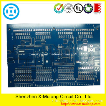
8L Bury & Blind Vias PCB, Impedance Control HDI PCB for Mobile Phone
- Payment Type:
- T/T, Net 30 days, net 45 days
Quantity:
Your message must be between 20 to 2000 characters
Contact NowBasic Info
Basic Info
| Place of Origin: | Shenzhen, China |
|---|---|
| Payment Type: | T/T, Net 30 days, net 45 days |
Product Description
Product Description
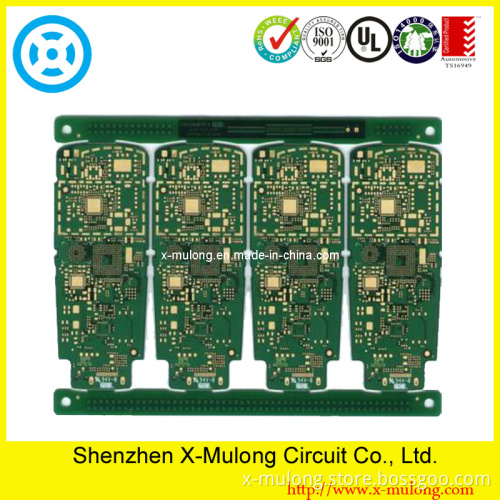
8L Bury & Blind Vias pcb, Impedance Control HDI PCB for Mobile Phone
Layer: 8L
Material: FR4 Laminate
PCB Thickness: 1.6mm+/-10%
Copper: 1oz for all layers
Min Hole: 0.2mm
Min line Width/Space: 5mil/5mil
Soldermask: Green
Legend: White
Surface: ENIG(immersion gold), Au thickness: Min. 3u"
Vias: Bury & blind via holes.
Other requires:Impedance control
E-Test: 100% E-testing by fixture
Outgoing Reports: Final Inspection Report, E-Test Report, Solderability Test Report, Microsection Report, PPAP and so on.
Inspection Standard: IPC-A-600H/IPC-6012B, Class 2/3
Certificates: UL, SGS, RoHS, ISO9001: 2008, ISO14001: 2004, ISO TS16949: 2009

Related Keywords
Related Keywords