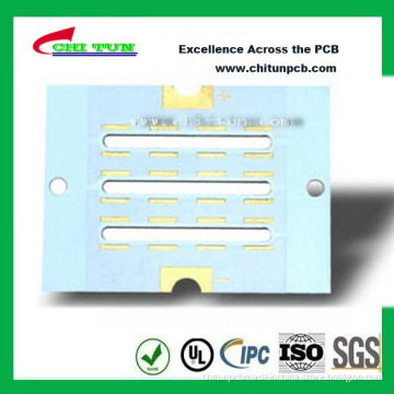
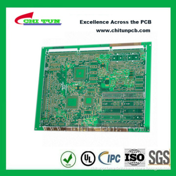
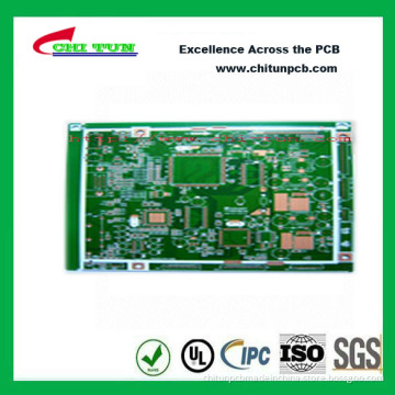
PCB of 4 Layer OSP Printed Circuit Board
- Payment Type:
- L/C, T/T, D/P, Paypal, Money Gram, Western Union
Quantity:
Your message must be between 20 to 2000 characters
Contact NowBasic Info
Basic Info
| Place of Origin: | CN |
|---|---|
| Payment Type: | L/C, T/T, D/P, Paypal, Money Gram, Western Union |
Product Description
Product Description
Part. No. CTE-012
Layers: 4Layer
Surface Finished: OSP
Material: FR4
Thickness: 1.6MM
Board Size: 245*180MM
Minimum Wire Width≥ : 3.5MIL
Smallest finish hole size: 8MIL
Finished copper: 1OZ
Solder Mask colour: Green
Peelable Soldermask: No
Silkscreen colour: White
CNC
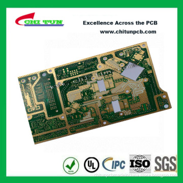
Standard: IPC-A-600G Class II/III
Certificates: UL/94V-0/ISO
TECHNOLOGY:
. RoHS/ Lead Free
. HDI Microvias
. Blind Vias
. Buried Vias
. Selective Plating
. Impedance Control
Manufacturing Standard:
. IPC-A-600G Class II
. IPC-A-600G Class III
. PERFAG 2E for Double-Sided Board
. PERFAG 3C for Multilayer Board
Capability
Min. Finished Holes Size: 0.008" (0.20mm)
Micro vias diameter: 0.004 TO 0.010 inches (0.10 - 0.25mm)
Minimum line width/spacing: 0.004/0.004 inches (0.10mm/ 0.10mm)
Maximum copper thickness: 5oz (140um)
Thin board thickness:
. DS - 0.008 inches (0.20mm)
. 4/L - 0.016 (0.40mm)
. 6/L - 0.020 inches (0.60mm)
Maximum board thickness:
. 275.8mil (7.0mm)
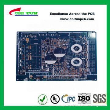
Surface treatment:
. HASL/lead free HAL/gold plating
. Immersion gold
. Immersion tin
. Immersion silver
. Gold fingers (hard gold)
. OSP
Other:
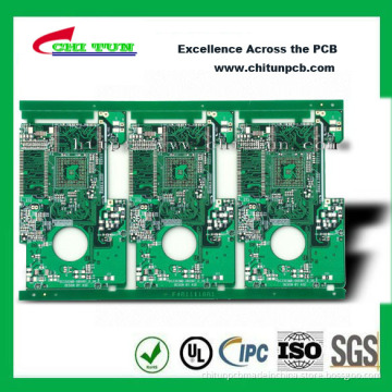
. Account of layers: Double-side to above 20 layers (1 to 30 layers)
. Max PCB dimensions: 23 x 35 inches (584.2 x 889.0mm)
. Solder mask bridge between solder dam: 4mil (0.10mm)
. Minimum solder mask annular: 1.5mil (0.038mm)
. Min thickness of solder mask: 0.40mil (10um)
. Solder mask colors: Green, yellow, black, blue, matte, transparence LPI solder mask and peelable solder mask
. Min height of Legend: 4mil (0.10mm)
. Min width of front: 25mil (0.635mm)
. Legend colors: White, yellow, black
Data format: GERBER, PROTEL, PADS2000, Powerpcb, ODB++
Special material: HTG FR4, high frequency (Rogers, Teflon, ARLON, TYCONIC), halogen free, different material mixing laminating
Other test: Impendence control, resistor of hole test, micro section, ionic cleanliness test, Soldering capacity, thermal shocking, reliability test, etc.
Layers: 4Layer
Surface Finished: OSP
Material: FR4
Thickness: 1.6MM
Board Size: 245*180MM
Minimum Wire Width≥ : 3.5MIL
Smallest finish hole size: 8MIL
Finished copper: 1OZ
Solder Mask colour: Green
Peelable Soldermask: No
Silkscreen colour: White
CNC
Standard: IPC-A-600G Class II/III
Certificates: UL/94V-0/ISO
TECHNOLOGY:
. RoHS/ Lead Free
. HDI Microvias
. Blind Vias
. Buried Vias
. Selective Plating
. Impedance Control
Manufacturing Standard:
. IPC-A-600G Class II
. IPC-A-600G Class III
. PERFAG 2E for Double-Sided Board
. PERFAG 3C for Multilayer Board
Capability
Min. Finished Holes Size: 0.008" (0.20mm)
Micro vias diameter: 0.004 TO 0.010 inches (0.10 - 0.25mm)
Minimum line width/spacing: 0.004/0.004 inches (0.10mm/ 0.10mm)
Maximum copper thickness: 5oz (140um)
Thin board thickness:
. DS - 0.008 inches (0.20mm)
. 4/L - 0.016 (0.40mm)
. 6/L - 0.020 inches (0.60mm)
Maximum board thickness:
. 275.8mil (7.0mm)
Surface treatment:
. HASL/lead free HAL/gold plating
. Immersion gold
. Immersion tin
. Immersion silver
. Gold fingers (hard gold)
. OSP
Other:
. Account of layers: Double-side to above 20 layers (1 to 30 layers)
. Max PCB dimensions: 23 x 35 inches (584.2 x 889.0mm)
. Solder mask bridge between solder dam: 4mil (0.10mm)
. Minimum solder mask annular: 1.5mil (0.038mm)
. Min thickness of solder mask: 0.40mil (10um)
. Solder mask colors: Green, yellow, black, blue, matte, transparence LPI solder mask and peelable solder mask
. Min height of Legend: 4mil (0.10mm)
. Min width of front: 25mil (0.635mm)
. Legend colors: White, yellow, black
Data format: GERBER, PROTEL, PADS2000, Powerpcb, ODB++
Special material: HTG FR4, high frequency (Rogers, Teflon, ARLON, TYCONIC), halogen free, different material mixing laminating
Other test: Impendence control, resistor of hole test, micro section, ionic cleanliness test, Soldering capacity, thermal shocking, reliability test, etc.
Related Keywords
Related Keywords
You May Also Like
You May Also Like