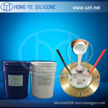
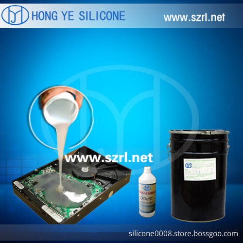
PCB Electronic Potting Silicone
- Payment Type:
- T/T
- Incoterm:
- FOB
- Min. Order:
- 200 Kilogram
- Min. Order:
- 200 Kilogram
- Delivery Time:
- 3 Days
- Transportation:
- Ocean
Your message must be between 20 to 2000 characters
Contact Now| Place of Origin: | Shenzhen |
|---|---|
| Productivity: | 8 tons per day |
| Supply Ability: | 8 tons per day |
| Payment Type: | T/T |
| Incoterm: | FOB |
| Transportation: | Ocean |
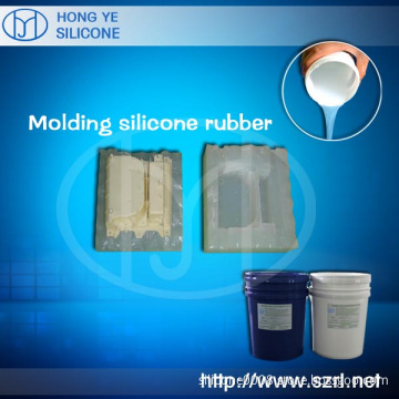
1.Application:
-Applying for the surface of PC,PP,ABS,PVC,metal
-Potting for the Protection of general electronic module
-Insulation,waterproof and bonding of electronics parts
-Filling for LED,LCD electronic display,circuit board
-Outdoor protection for LED screen.
2.Characteristics: Low viscosity,easy pouring operation ,and good bonding feature.It can be cured completely at room temprature.The safety of potting compound silicone can reach the EU-ROHS requirements fully.
3.Technical Guidelines
1. Pls put part A and B in separate container and stir evenly before mixing the two
parts together.
2. Mixing Ratio part A:part B is 10:1
3. Bubble release if necessary, deaeration the mixture under 0.08 MPa for 3 minutes.
4. HY-215# is cured at roon temperature, so pls put it under room temperature after
pouring. It comes to next process when basically cured, and it takes about 24 hours
for completely cured
4. Warm Tips for for PCB Electronic Potting Silicone
1. Sealing pakage for storage. The mixture should be used up at once to avoid wasting.
2. Silicone belongs to non-dangerous goods, but keep away form mouth and eyes.
3. When it gets stratified after a period of storage, Please mix HY-210# evenly before using,
it does not affect the performance.


Related Keywords