


High Quality Shenzhen Single Layer Pcb Pcba Manufacturer
Quantity:
Your message must be between 20 to 2000 characters
Contact NowBasic Info
Basic Info
Product Description
Product Description
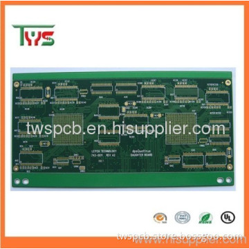
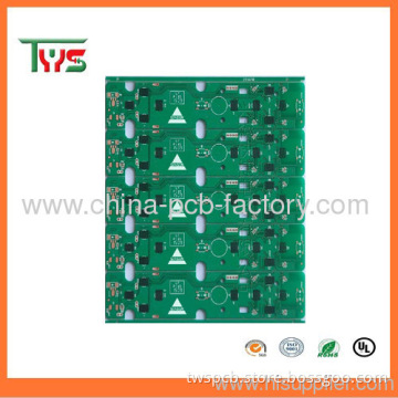
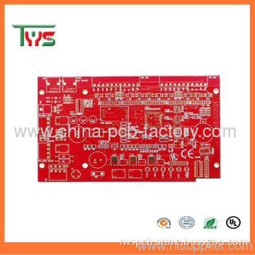
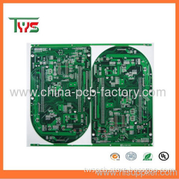
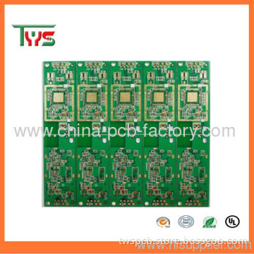
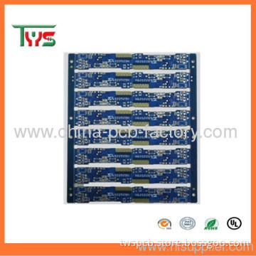
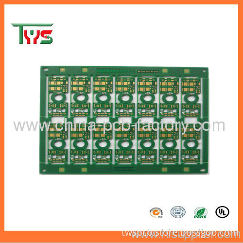
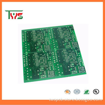
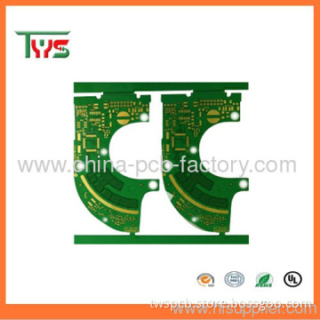
shenzhen pcb pcba manufacturer
Shenzhen pcb pcba manufacturer
Shenzhen Tianweisheng Electronics Co., Ltd. is a professional PCB printed circuit board manufacturer. Our production base is located in Bao'an with convenient communication facilities. Our company covers an area of 8, 000 square meters and has more than 300 employees, among whom 80% are senior staff members.
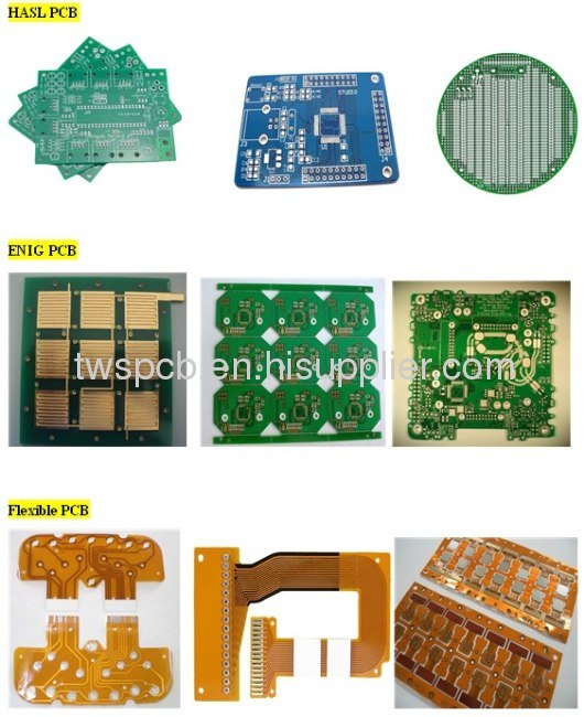
Since established, we have been committed to the professional high-precision single-double-sided and multi-layer printed circuit board manufacture. Our company always concerns about the PCB industry to get new technologies and control to advance with the times. We always adhere to using advanced concepts and mature sound technical production to better meet the needs of market. Through unremitting efforts, our R&D team now manufacture multilayer blinds, buried hole circuit boards, flexible circuit boards (FPC), high-precision impedance, HDI, and other special circuit boards. Fast delivery, high quality and reliable credibility are our company's first comparative advantage which will be able to offer customers real models for single, double-sided 12-24 hours intensive, 4-8 layer-48-72 hours of quick PCB and small quantities of Rapid Plate services.
Our advantages
1.Professional engineer can provide PCB circuit design,BOM and diagram drawings.
2.Provide PCB &PCBA prototype manufacturing, and medium&low volume quick board services.
3.Compoent purchasing, SMT/PCBA one-stop source, with the professional purchasing team
4.One-hour quote response, 24 hours quick-turn produce
5.Variety terms of delivery,customize the flexibility to choose
Detailed specification of manufaturing capacity:
NO |
Item |
Craft Capacity |
1 |
Layer |
1-30 Layers |
2 |
Base Material for PCB |
FR4, CEM-1, TACONIC, Aluminium, High Tg Material, High Frequence ROGERS ,TEFLON, ARLON, Halogen-free Material |
3 |
Rang of finish baords Thickness |
0.21-7.0mm |
4 |
Max size of finish board |
900MM*900MM |
5 |
Minimum Linewidth |
3mil (0.075mm) |
6 |
Minimum Line space |
3mil (0.075mm) |
7 |
Min space between pad to pad |
3mil (0.075mm) |
8 |
Minimum hole diameter |
0.10 mm |
9 |
Min bonding pad diameter |
10mil |
10 |
Max proportion of drilling hole and board thickness |
1:12.5 |
11 |
Minimum linewidth of Idents |
4mil |
12 |
Min Height of Idents |
25mil |
13 |
Finishing Treatment |
HASL (Tin-Lead Free), ENIG(Immersion Gold), Immersion Silver , Gold Plating (Flash Gold), OSP, etc. |
14 |
Soldermask |
Green, White, Red, Yellow, Black, Blue, transparent photosensitive soldermask, Strippable soldermask. |
15 |
Minimun thickness of soldermask |
10um |
16 |
Color of silk-screen |
White, Black, Yellow ect. |
17 |
E-Testing |
100% E-Testing (High Voltage Testing); Flying Probe Testing |
18 |
Other test |
ImpedanceTesting,Resistance Testing, Microsection etc., |
19 |
Date file format |
GERBER FILE and DRILLING FILE, PROTEL SERIES, PADS2000 SERIES, Powerpcb SERIES, ODB++ |
20 |
Special technological requirement |
Blind & Buried Vias and High Thickness copper |
21 |
Thickness of Copper |
0.5-14oz (18-490um) |
Shenzhen pcb pcba manufacturer

Related Keywords
Related Keywords