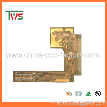


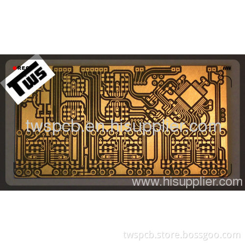
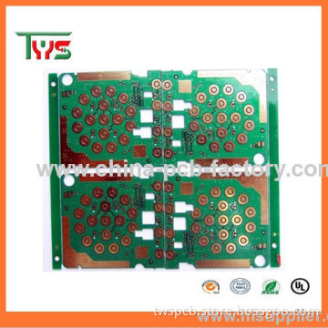
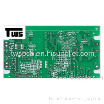
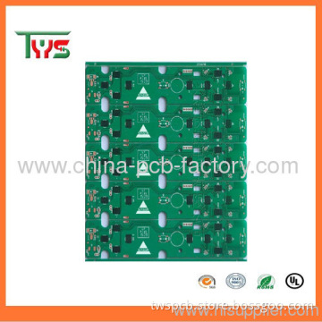
Bare Pcb For Mobile Phone Motherboard
Quantity:
Your message must be between 20 to 2000 characters
Contact NowBasic Info
Basic Info
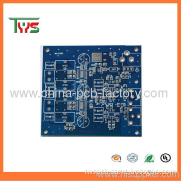
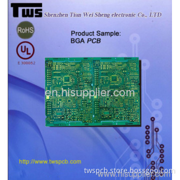
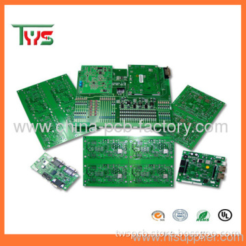
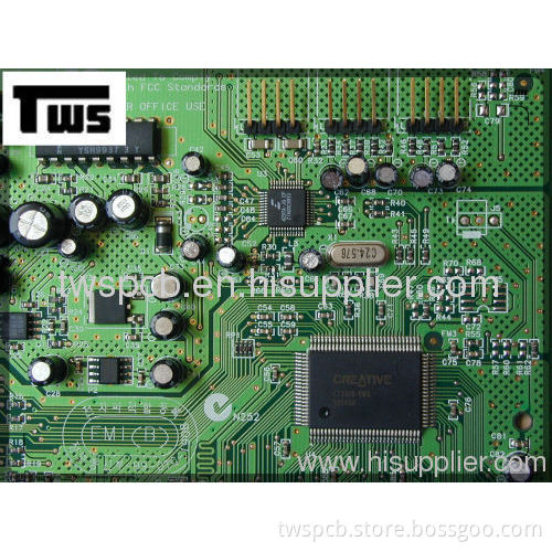
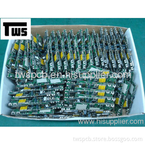
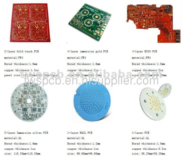
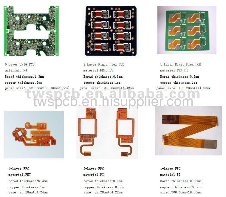
Product Description
Product Description
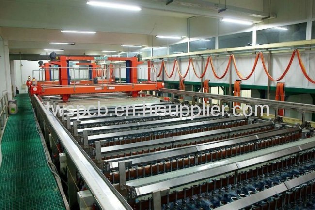
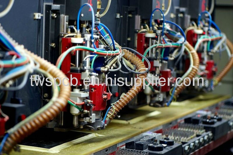
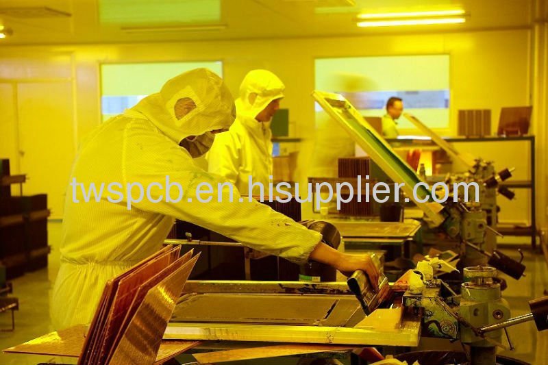
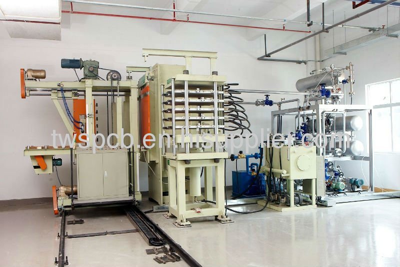
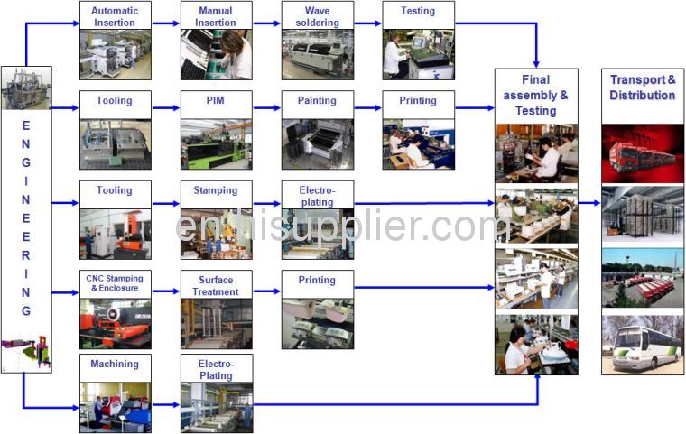
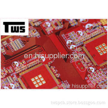
Advanced ProductionEquipment
Product HighQuality Perfect
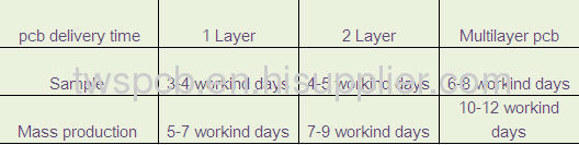
Our deliverytime:
1.About Factory:
Experience: we have 20 years experinecsin circuit board manufacturing,with 50 employees and 60 excellent engineers,covering an area of 13000 square meters.Monthly capability is more than 5000square meters, 4500 types/month. we cooperate with some well-known enterprises,such as Panasonic, HP,Honeywell and so on.
2.Good after sales service:
anything wrong happening in our products willbe solved within 2 hours. we always offer relative technical support/consultant.Quick response. all your inquiry will be replied within 24 hours.
3.Ourproducts and service are sold well in North America,West Europe, Japan,Singpore, Malaysia and other countries.
Meet your need is ourgreatest pursuit .If you are looking for a pcb board manufacturerinchina,Pleasegive us your files ofpcb for a quote (Gerberfiles and specification),I will reply email in 3hours. Youalso cancontact usby .
1.Advanced production lines andprofessional staff.
2.Honesty credibility in china'stop.
3.Competest price but highquality.
4. One-stopservice.
5.Delivery ontime.
NO |
Item |
Craft Capacity |
1 |
Layer |
1-30 Layers |
2 |
Base Material for PCB |
FR4, CEM-1, TACONIC, Aluminium, High Tg Material, High Frequence ROGERS ,TEFLON, ARLON, Halogen-free Material |
3 |
Rang of finish baords Thickness |
0.21-7.0mm |
4 |
Max size of finish board |
900MM*900MM |
5 |
Minimum Linewidth |
3mil (0.075mm) |
6 |
Minimum Line space |
3mil (0.075mm) |
7 |
Min space between pad to pad |
3mil (0.075mm) |
8 |
Minimum hole diameter |
0.10 mm |
9 |
Min bonding pad diameter |
10mil |
10 |
Max proportion of drilling hole and board thickness |
1:12.5 |
11 |
Minimum linewidth of Idents |
4mil |
12 |
Min Height of Idents |
25mil |
13 |
Finishing Treatment |
HASL (Tin-Lead Free), ENIG(Immersion Gold), Immersion Silver , Gold Plating (Flash Gold), OSP, etc. |
14 |
Soldermask |
Green, White, Red, Yellow, Black, Blue, transparent photosensitive soldermask, Strippable soldermask. |
15 |
Minimun thickness of soldermask |
10um |
16 |
Color of silk-screen |
White, Black, Yellow ect. |
17 |
E-Testing |
100% E-Testing (High Voltage Testing); Flying Probe Testing |
18 |
Other test |
ImpedanceTesting,Resistance Testing, Microsection etc., |
19 |
Date file format |
GERBER FILE and DRILLING FILE, PROTEL SERIES, PADS2000 SERIES, Powerpcb SERIES, ODB++ |
20 |
Special technological requirement |
Blind & Buried Vias and High Thickness copper |
21 |
Thickness of Copper |
0.5-14oz (18-490um) |
Related Keywords
Related Keywords
You May Also Like
You May Also Like