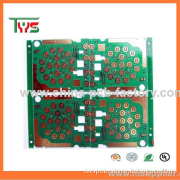


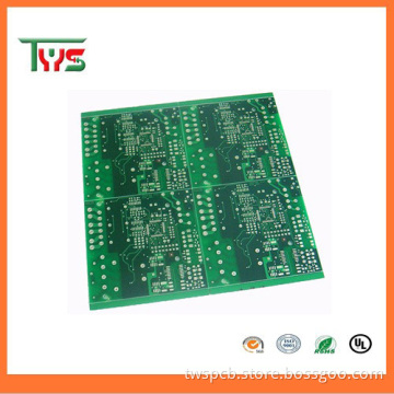
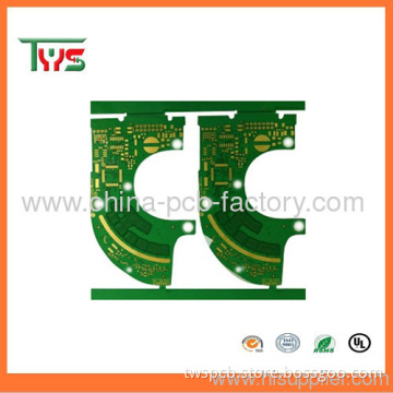
4 Layers Printed Circuit Board With Odm/oem Service
Quantity:
Your message must be between 20 to 2000 characters
Contact NowBasic Info
Basic Info
Product Description
Product Description
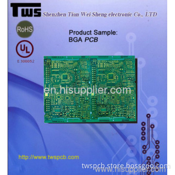
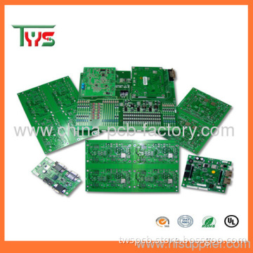
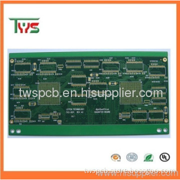
4 layers printed circuit board
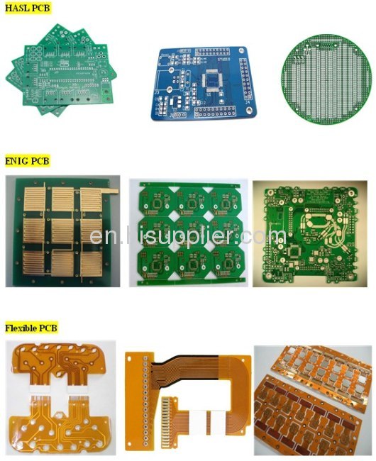
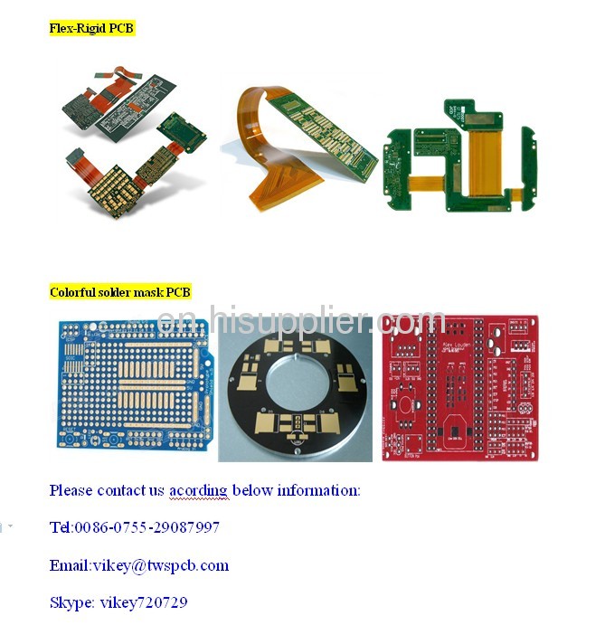
Layer:1~18 layers
Materials: FR-4, CEM-3, Teflon, Aluminum, Rogers, High Tg
Surface finished:Lead Free HASL,Immersion Gold/Tin/Silver, OSP, Gold Finger Plating, Selective Immersion Gold,Gold Plating.
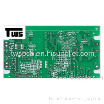
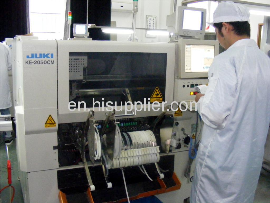
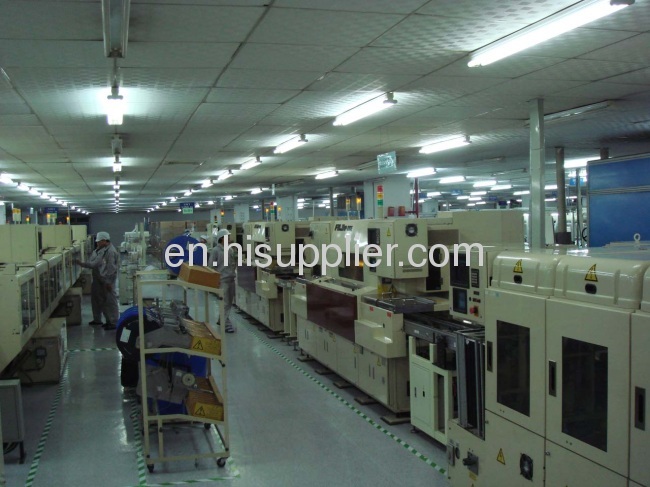
PCB assembly
Military standard assembly
PCB assembly
Military standard assembly
Minimum lead time for assembly is only 3 days
Turnkey service(PCB manufacture, components procurement and assembly)
Prototype building, No Minimum quantity Required
Reliable Parts
Surface mount, through hole, BGA, QFP, QFN …
ROHS compliant and lead-free process
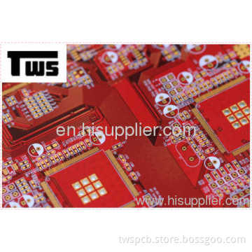
♣ High layers PCB manufacturing, up to 32 layers
♣ Low costs, Minimum cost for 3 prototype boards is only $84!!!
♣ Fast service, Minimum lead time for bare PCB is only 2 days
♣ Promptly reply, quotation will be provided in 8 working hours!
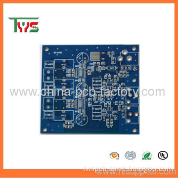
Our PCBs are used for wide range of electronic products,
Like WIFI, Medical devices, CCTV, Power supply, GPS, UPS, Set-top Box,
Telecomunication ,LED, etc.
Technical Specifications
English |
Metric |
|||
1 |
Max. Panel Size |
22" x 26" |
550 x 650mm |
|
2 |
Mechanical Drill |
|||
Min. Finished Holes Size |
0.004" |
0.10mm |
||
Finished Holes Tolerance |
PTH |
±0.003" |
±0.075mm |
|
NPTH |
±0.002" |
±0.050mm |
||
Press Fit |
±0.002" |
±0.050mm |
||
Aspect Ratio |
9 : 1 |
9 : 1 |
||
3 |
Laser Drill |
|||
Microvias diameter |
0.004" - 0.006" |
0.10 - 0.15mm |
||
Aspect Ratio |
1 : 1 |
1 : 1 |
||
4 |
Min. Line Width/Spacing |
½oz / 18um |
0.003" / 0.003" |
0.075 / 0.075mm |
1oz / 35um |
0.006" / 0.006" |
0.15 / 0.15mm |
||
2oz / 70um |
0.008" / 0.008" |
0.20 / 0.20mm |
||
3oz / 105um |
0.010" / 0.010" |
0.25 / 0.25mm |
||
5 |
Registration |
|||
Solder Mask |
±0.003" |
±0.075mm |
||
Layer to Layer |
±0.0024" |
±0.060mm |
||
Copper Feature to Holes(Outer) |
±0.003" |
±0.075mm |
||
Min. Plated Drills to Copper (inner) |
2L - 8L |
0.010" |
0.25mm |
|
10L -22L |
0.012" |
0.30mm |
||
6 |
Board Outline |
|||
Edge to Edge Tolerance |
±0.004" |
±0.10mm |
||
Holes to Edge Tolerance |
±0.004" |
±0.100mm |
||
Min. Copper to Edge distance |
Outer |
0.010" |
0.25mm |
|
Inner |
0.016" |
0.40mm |
||
7 |
Max. Copper Thickness |
4oz |
140μm |
|
8 |
Max. Board Thickness |
0.189" |
4.80 mm |
|
9 |
Min Board Thickness |
2L |
0.008" |
0.20mm |
4L |
0.016" |
0.40mm |
||
6L -22L |
0.020" |
0.60mm |
||
10 |
Min. Core Thickness |
0.004" |
0.10mm |
|
11 |
Min. Soldermask Dam |
0.004" |
0.10mm |
|
12 |
Controlled Impedance (Ohm) |
±7% - 10% |
±7% - 10% |
|

Related Keywords
Related Keywords