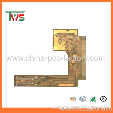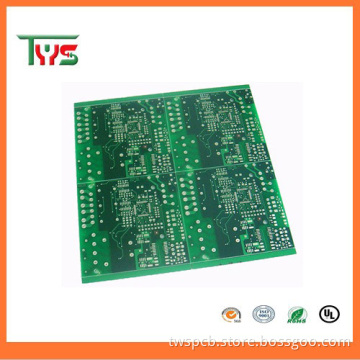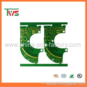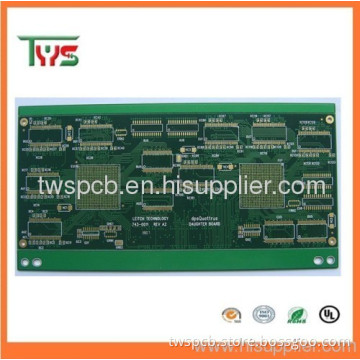


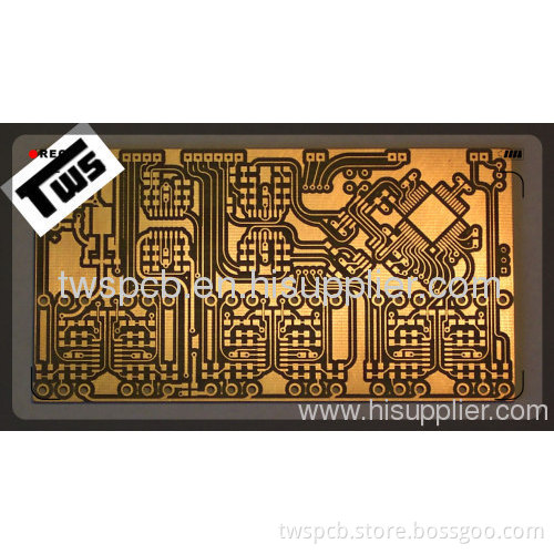
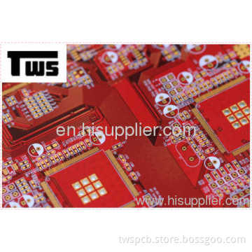
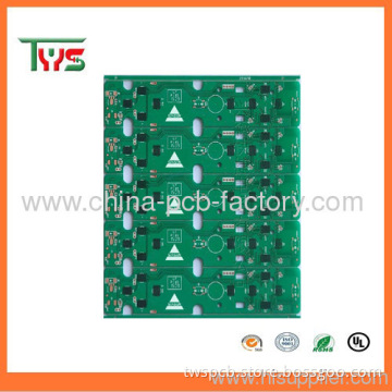
Double Layer Pcb Substrate Fr4 Pcb
Quantity:
Your message must be between 20 to 2000 characters
Contact NowBasic Info
Basic Info
Product Description
Product Description
Quick Details
| Place ofOrigin: | Guangdong China (Mainland) | BrandName: | XingDa | Number ofLayers: | 4-Layer |
| Base Material: | FR-4,FR2.Taconic,Rogers,CEM-1 CEM-3,ceramic , crockery Metal-backed L |
Copper Thickness: | 1/2 oz min;12 oz max | Board Thickness: | 0.2mm-6.00 mm(8mil-126mil) |
| Min. Hole Size: | 0.1mm(4mil) | Min. Line Width: | 0.075mm(3mil) | Min. Line Spacing: | 0.1mm4mil) |
| Surface Finishing: | ImmersionGold/Au,HASL,OSP,etc. |
Warp & Twist:: | 0.7% | Hole Positon: | +/-0.075mm(3mil) CNC Driling |
| Insulation Resistance: | 10Kohm-20Mohm | Conductivity: | <50ohm | Test Voltage: | 10-300V |
| ance Control: | +/-10% | Different Impendance: | +-/10% | Outline Tolerance: | 0.125mm(5mil) CNCRouting;+/-0.15mm(6mil) by Punching |
| Hole Diameter(H): | PTHL:+/-0.075mm(3mil);Non-PTH L:+/-0.05mm(2mil) |
Conductor Width(W): | +/-20% of originalartwork PTH L:+/-0.075mm(3mil) |
Packaging & Delivery
| Packaging Detail: | PCB: 5-10 days; PCBA:20-25 days |
| Delivery Detail: | 1. at buyer's request 2. inner, vacuum package 3. outer, standar |
Specifications
1.Competitive price
2.Prompt Reply&Delivery
3.High quality,Best service
4.ISO9001/TS16949/ROHS
2.Prompt Reply&Delivery
3.High quality,Best service
4.ISO9001/TS16949/ROHS
Welcome to XingDa Electric TechnologyCo.,Ltd
Xindaxing Electric TechnologyCo.,LTd
Weare professionalmanufacturer in various PCB and PCBA with many yearsexperience,We can provide a reasonable price with high quality products.
XingDa who canprovide a full set of service.such asbelow:
*1. PCB layout, PCB design
* 2: Make high difficultyPCB(1 to 38 layers)
* 3: Provide all Electroniccomponents
*4: PCB assembly
*5: Write programs for clients
* 6:PCBA/finished product Test. etc.
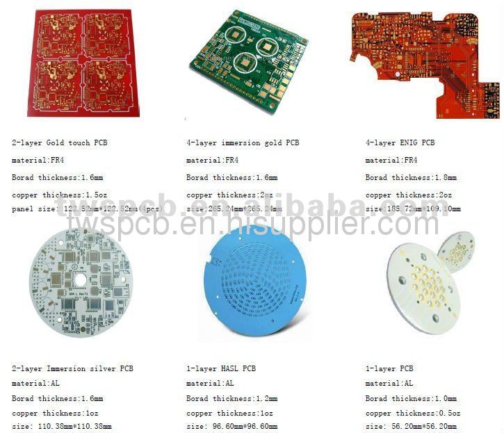
1.PCB Specificationdetail.
| Item | Specification | |
| 1 | Numbr ofLayer | 1-38Layers |
| 2 | Material | FR-4,FR2.Taconic,Rogers, CEM-1 CEM-3,ceramic , crockery Metal-backedLaminate |
| 3 | FinishBoard Thickness | 0.2mm-6.00mm(8mil-126mil) |
| 4 | Minimun CoreThickness | 0.075mm(3mil) |
| 5 | CopperThickness | 1/2 oz min;12oz max |
| 6 | Min.TraceWidth & Line Spacing | 0.075mm/0.1mm(3mil/4mil) |
| 7 | Min.HoleDiameter for CNC Driling | 0.1mm(4mil) |
| 8 | Min.HoleDiameter for punching | 0.9mm(35mil) |
| 9 | Biggest panelsize | 610mm*508mm |
| 10 | HolePositon | +/-0.075mm(3mil)CNC Driling |
| 11 | ConductorWidth(W) | 0.05mm(2mil)or;+/-20%of original artwork |
| 12 | HoleDiameter(H) | PTHL:+/-0.075mm(3mil);Non-PTH L:+/-0.05mm(2mil) |
| 13 | OutlineTolerance | 0.125mm(5mil)CNC Routing;+/-0.15mm(6mil) by Punching |
| 14 | Warp &Twist | 0.70% |
| 15 | InsulationResistance | 10Kohm-20Mohm |
| 16 | Conductivity | <50ohm |
| 17 | TestVoltage | 10-300V |
| 18 | PanelSize | 110×100mm(min);660×600mm(max) |
| 19 | Layer-layermisregistration | 4layers:0.15mm(6mil)max;6 layers:0.25mm(10mil)max |
| 20 | Min.spacingbetween hole edge to circuity pqttern of an inner layer | 0.25mm(10mil) |
| 21 | Min.spacingbetween board oulineto circuitry pattern of an inner layer | 0.25mm(10mil) |
| 22 | Boardthickness tolerance | 4layers:+/-0.13mm(5mil);6 layers:+/-0.15mm(6mil) |
| 23 | ImpedanceControl | +/-10% |
| 24 | DifferentImpendance | +-/10% |
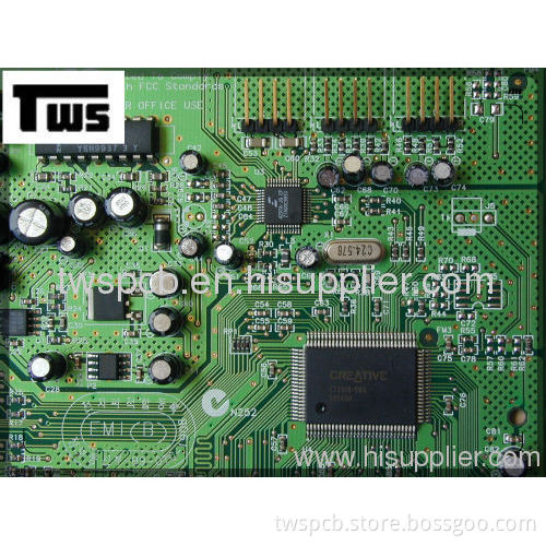
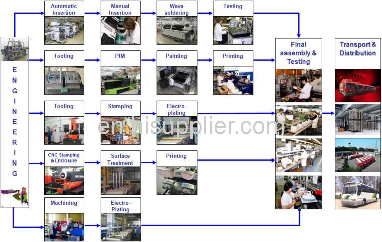
2.Details forPCB Assembly
Technical
1).Professionalsurface mounting and through hole soldering technology;
2).Varioussizes,like 1206,0805,0603 components SMT technology;
3).ICT(InCircuit Test),FCT(Functional Circuit Test) technology;
4).Nitrogengas reflow soldering technology for SMT;
5).Highstandard SMT&Solder Assembly line;
6).Highdensity interconnected board placement technology capacity.
Quoterequirement
1).The detailed files(Gerberfiles,specification andBOM);
2).Clearpictures of PCBA or samples for us;
3).PCBATest method.
Product HighQuality Perfect
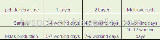
Our deliverytime:
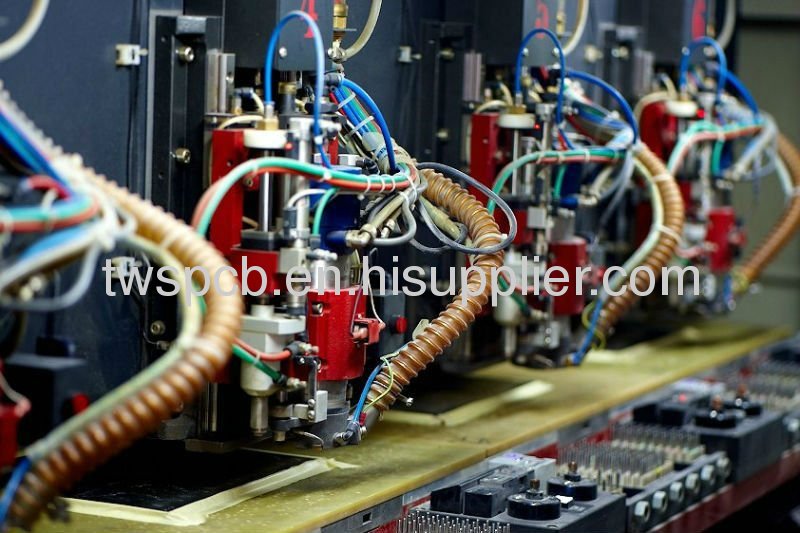
1.About Factory:
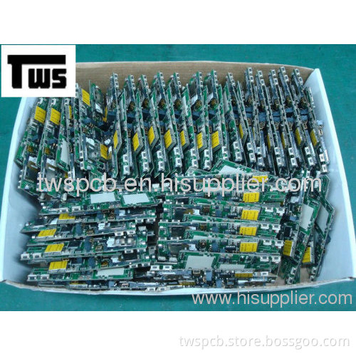
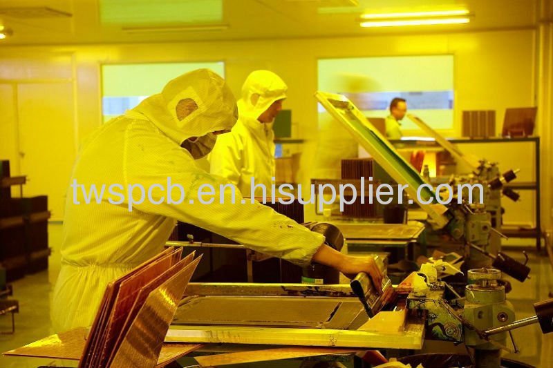
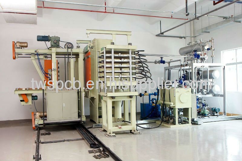
Experience: we have 20 years experinecsin circuit board manufacturing,with 50 employees and 60 excellent engineers,covering an area of 13000 square meters.Monthly capability is more than 5000square meters, 4500 types/month. we cooperate with some well-known enterprises,such as Panasonic, HP,Honeywell and so on.
2.Good after sales service:
anything wrong happening in our products willbe solved within 2 hours. we always offer relative technical support/consultant.Quick response. all your inquiry will be replied within 24 hours.
3.Ourproducts and service are sold well in North America,West Europe, Japan,Singpore, Malaysia and other countries.
Meet your need is ourgreatest pursuit .If you are looking for a pcb board manufacturerinchina,Pleasegive us your files ofpcb for a quote (Gerberfiles and specification),I will reply email in 3hours. Youalso cancontact usby .
1.Advanced production lines andprofessional staff.
2.Honesty credibility in china'stop.
3.Competest price but highquality.
4. One-stopservice.
5.Delivery ontime.
Related Keywords
Related Keywords
You May Also Like
You May Also Like