

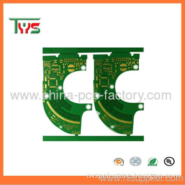
Double Side Flexible Pcb Design
Quantity:
Your message must be between 20 to 2000 characters
Contact NowBasic Info
Basic Info
Product Description
Product Description
Quick Details
| Place of Origin: | Guangdong China (Mainland) | Brand Name: | Chintech | Model Number: | pcb-004 |
| Number of Layers: | 2-Layer | Base Material: | FR4 TG150 | Copper Thickness: | 1.0 OZ |
| Board Thickness: | 1.6mm | Min. Hole Size: | 0.1mm | Min. Line Width: | 0.15mm |
| Min. Line Spacing: | 0.2mm | Surface Finishing: | Immersion Gold |
Packaging & Delivery
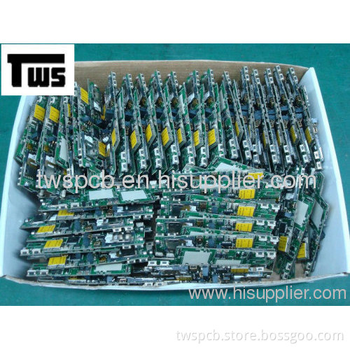
| Packaging Detail: | Vacuum package into carton |
| Delivery Detail: | 7~12 days |
Specifications
Double Side Flexible PCB Design
1.Base Material:FR4& Copper core
2.Thicknes:1.6mm
3.Copper thickness:1.0OZ
4.Vacuumpackage
1.Base Material:FR4& Copper core
2.Thicknes:1.6mm
3.Copper thickness:1.0OZ
4.Vacuumpackage
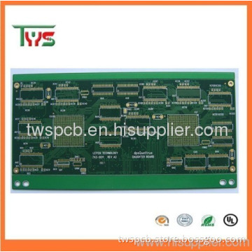
Double Side Flexible PCB Design
Specifications:
Printcircuit board design and assembly
Singlelayer and multiple layers board
All sizeand shape can be made With ISO9001/UL/RoHS marks
Smallquantity are accepted
Finequality and cheap price
Strictquality system
Highquality circuit board
Quick turn Strong engineeringsupport
Productlines:
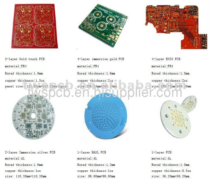
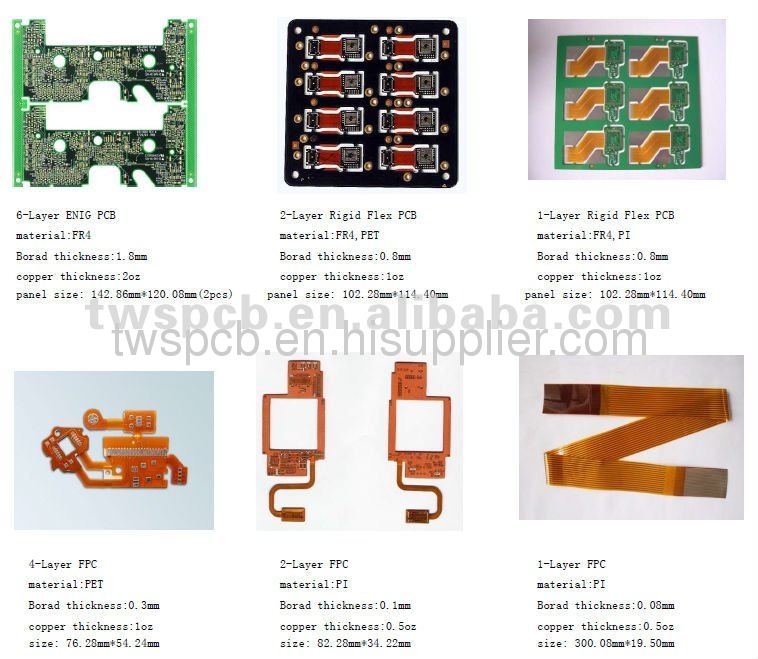
-RigidPCB( Single-sided PCB,Double-sided PCB,Multi-layer PCB-up to30layers)
-Rigid-flexiblePCB(1 to 16layers)
-FlexiblePCB(1 to 8layers)
-HDIPCB
-Allkinds of high class PCBs
PCBmaterial we can use:
FR1,FR2, HB,CEM1,CEM3, FR4,High TG/CTI FR4,Halogen Free,Rogers,Aluminium based,Leadfree compatible, Hi Frequency
Requested information for PCB assembly:
1.Gerber file of the bare PCB board
2. BOM (Bill of material) for assembly
3. Testing Guide & Test Fixtures if necessary
5. Schematic if necessary
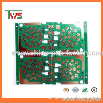
Double Side Flexible PCBDesign
OurTechnologyCapacity:
HDIPCB
2009 |
2010 |
2011 |
2012 |
|
Line width/Space |
3.0/3.0 mil |
2.5/2.5 mil |
2.0/2.0 mil |
2.0/2.0 mil |
Min. Micro Via(Unfinished) |
4.0mil |
3.5mil |
3.5mil |
3.0mil |
Max. Micro Via AspectRatio |
0.8:1 |
0.9:1 |
1:1 |
1:1 |
Min. Micro Via Pad |
11mil |
10mil |
10mil |
10mil |
Impedance Control |
±10% |
±8% |
±8% |
±7% |
Layer to Layer Reg |
±3.0 mil |
±2.5 mil |
±2.5 mil |
±2.0 mil |
S/M Reg |
±2.0 mil |
±2.0 mil |
±1.5 mil |
±1.0mil |
Min.Build-up DielectricThickness |
3.0mil |
2.5mil |
2.0mil |
2.0mil |
Max. Build-up |
2 |
3 |
4 |
4 |
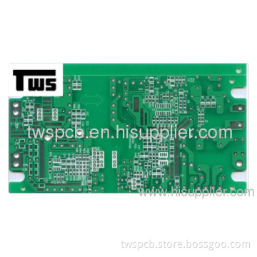
Product HighQuality Perfect
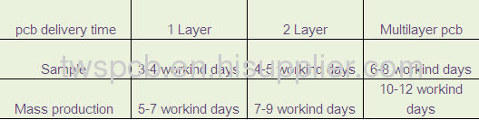
Our deliverytime:
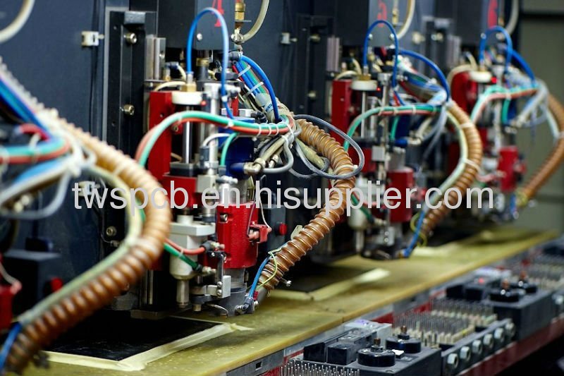
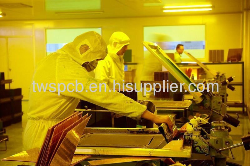
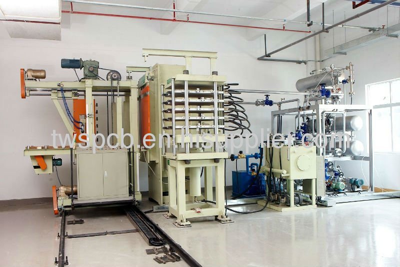
1.About Factory:
Experience: we have 20 years experinecsin circuit board manufacturing,with 50 employees and 60 excellent engineers,covering an area of 13000 square meters.Monthly capability is more than 5000square meters, 4500 types/month. we cooperate with some well-known enterprises,such as Panasonic, HP,Honeywell and so on.
2.Good after sales service:
anything wrong happening in our products willbe solved within 2 hours. we always offer relative technical support/consultant.Quick response. all your inquiry will be replied within 24 hours.
3.Ourproducts and service are sold well in North America,West Europe, Japan,Singpore, Malaysia and other countries.
Meet your need is ourgreatest pursuit .If you are looking for a pcb board manufacturerinchina,Pleasegive us your files ofpcb for a quote (Gerberfiles and specification),I will reply email in 3hours. Youalso cancontact usby .
1.Advanced production lines andprofessional staff.
2.Honesty credibility in china'stop.
3.Competest price but highquality.
4. One-stopservice.
5.Delivery ontime.
Related Keywords
Related Keywords